
What we do
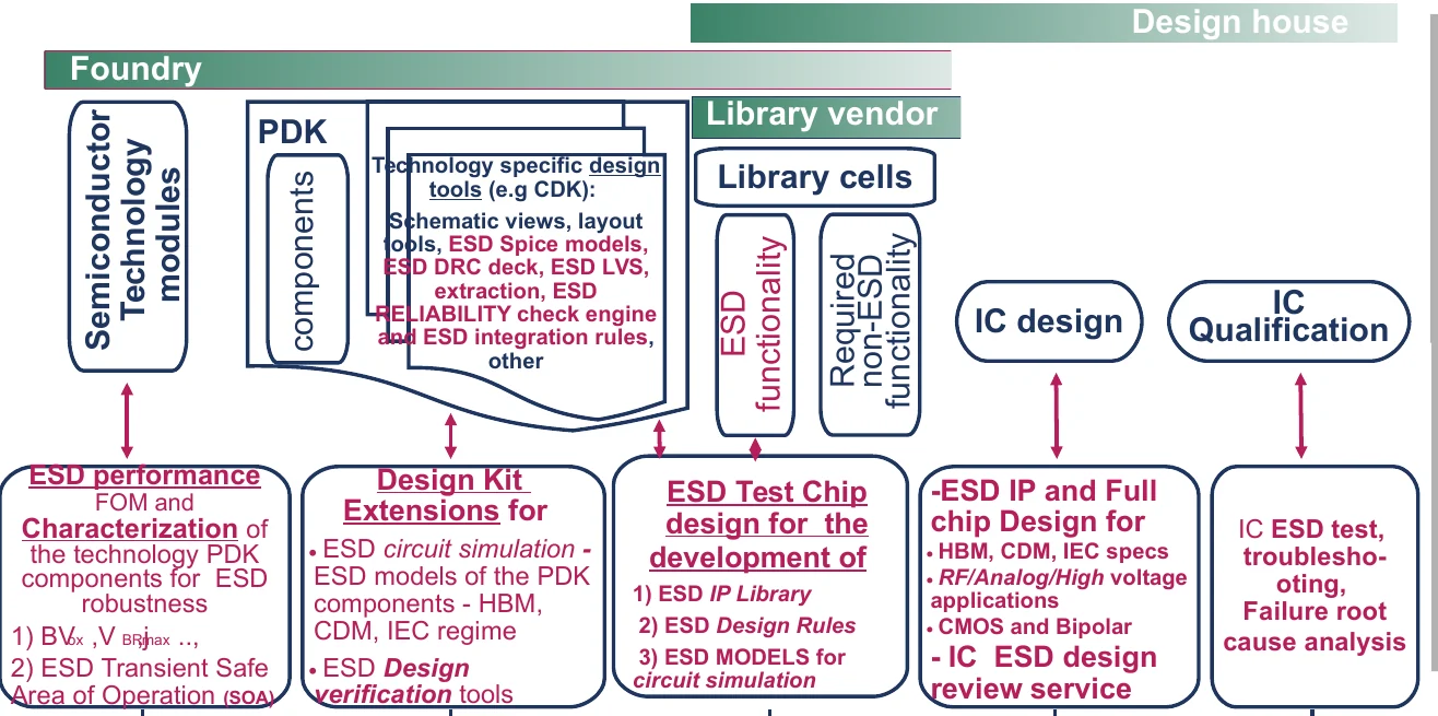
Every ESD-robust product starts with the technology. We characterize the safe area of operation of your components and turn the results into test chips, design rules and models.
- Semiconductor technology optimization for ESD reliability
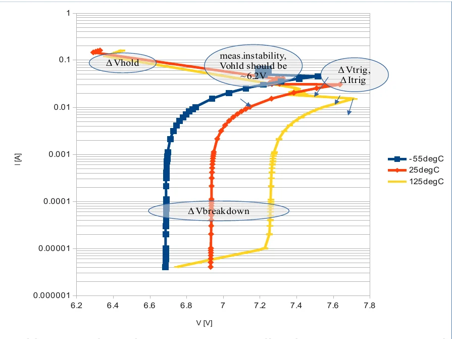
- ESD safe operating area (SOA) characterization of the components in your PDK: oxide and junction breakdown voltages, transient ESD SOA and figures of merit
- ESD test chip design to develop the ESD IP library, ESD design rules and ESD models for circuit simulation
- Transmission line pulse (TLP) characterization hardware for your test house
Who this is for
Semiconductor technology foundries and IDMs that want ESD-ready process technologies and design kits.
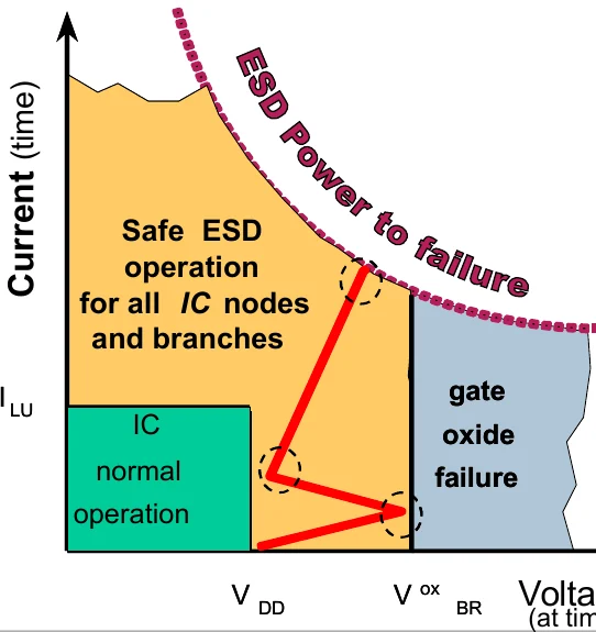
From device physics to design data
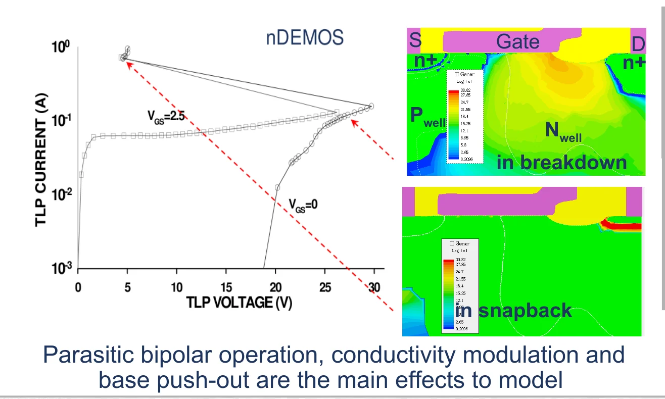
We combine measurement, TCAD and compact modeling to understand the effects that decide ESD performance.
Tell us about your ESD challenge
Send a short description of your technology, product or failure and we will tell you how we would approach it.