Real ESD design problems, solved with calibrated models, simulation and measurement. Select a figure to enlarge it.
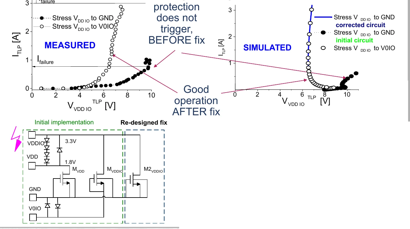
Power-supply pad that never triggered
Digital and mixed-signal
High-voltage
1.8 V core, 3.3 V I/O
Measured TLP data showed the protection did not trigger. SPICE simulation reproduced the behavior, and the re-designed cell with an added device worked as predicted. Measured and simulated curves correlate closely.
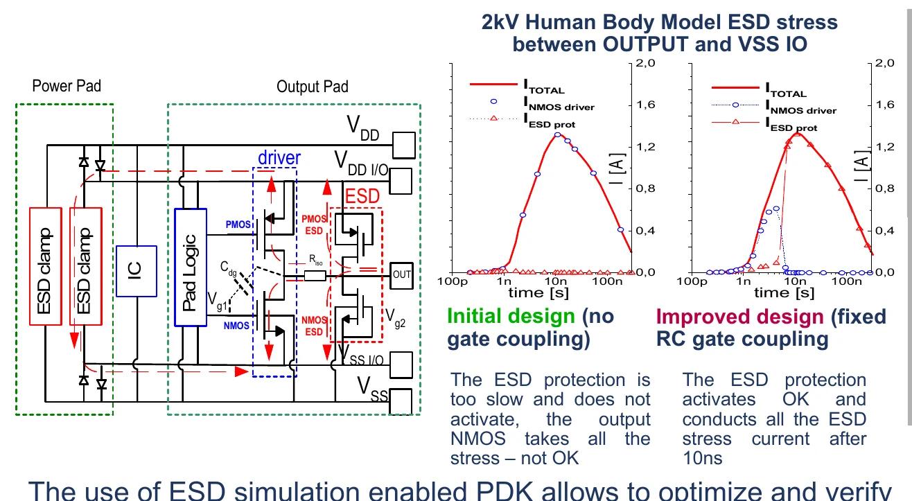
Digital output pad: protection too slow
Digital and mixed-signal
HBM 2 kV
With no gate coupling the ESD clamp was too slow and the output NMOS took all the stress. Adding RC gate coupling made the protection conduct the whole ESD current after 10 ns.
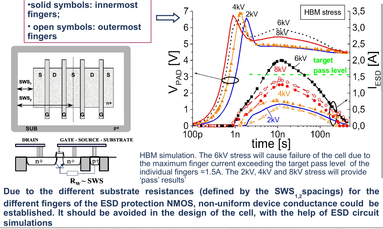
Non-uniform finger activation
Digital and mixed-signal
HBM simulation
Different substrate resistances across the fingers of an ESD NMOS made them conduct unevenly. Simulation showed that at 6 kV the busiest finger exceeded the 1.5 A pass level, while 2, 4 and 8 kV passed.
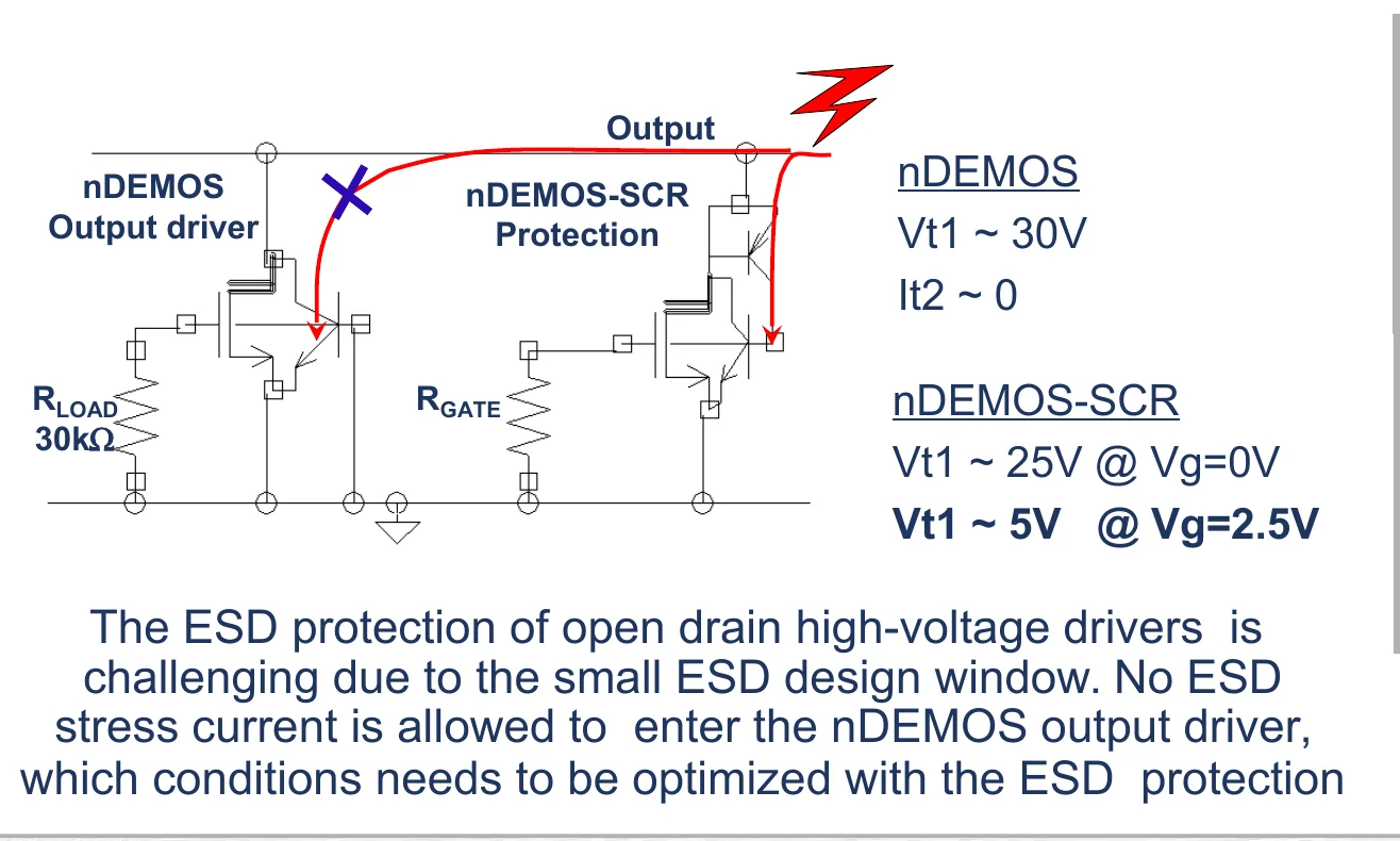
Open-drain high-voltage driver
High-voltage
nDEMOS-SCR
The small ESD design window means no stress current may enter the nDEMOS output driver. An nDEMOS-SCR clamp triggers at about 25 V with no gate bias and about 5 V with 2.5 V on the gate, against about 30 V for the nDEMOS alone.
Tuning the trigger of a power output cell
High-voltage
HBM 2 kV
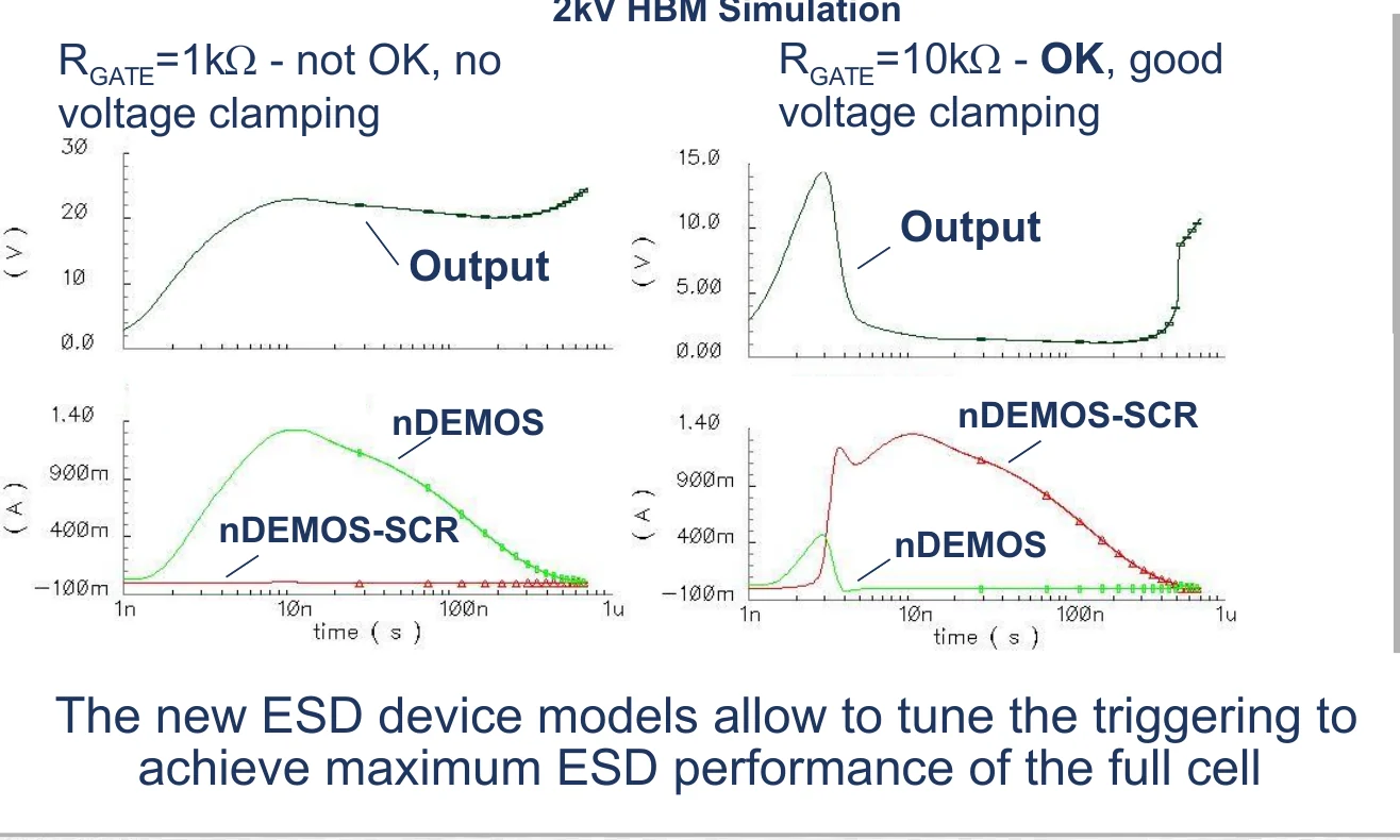
In a 2 kV HBM simulation, a 1 kΩ gate resistor gave no voltage clamping, while 10 kΩ clamped well and moved the ESD current into the SCR protection.
Trigger speed and voltage overshoot
High-voltage
HBM 1 kV
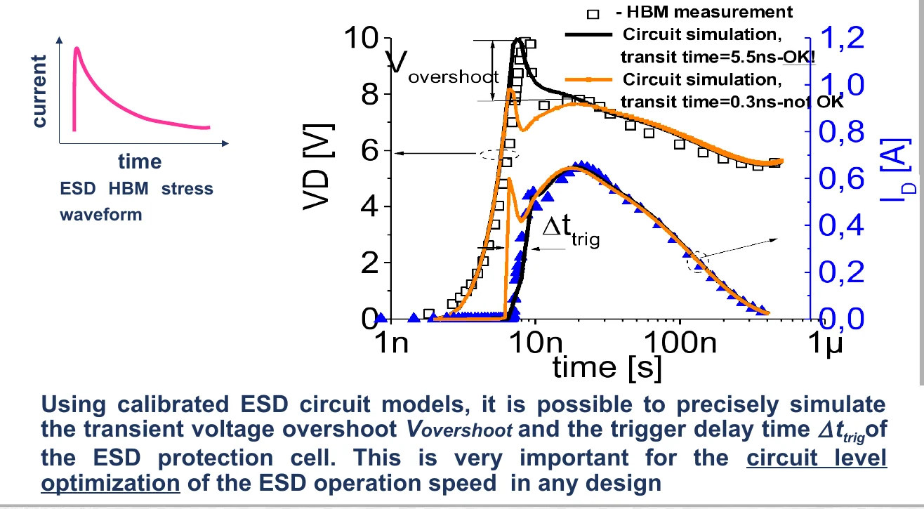
Calibrated circuit models reproduce the measured voltage overshoot and trigger delay of a high-voltage protection cell. This is what lets designers optimize ESD operation speed at circuit level.
nDEMOS snapback model validation
High-voltage
DC measurement and simulation
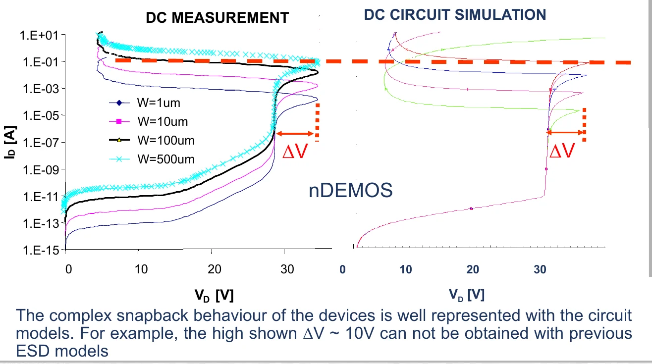
The complex snapback of nDEMOS devices is well represented by our circuit models. The snapback ΔV of about 10 V cannot be obtained with previous ESD models.
5 V-tolerant I/O in 3.3 V CMOS
Digital and mixed-signal
Cascoded ESD NMOS
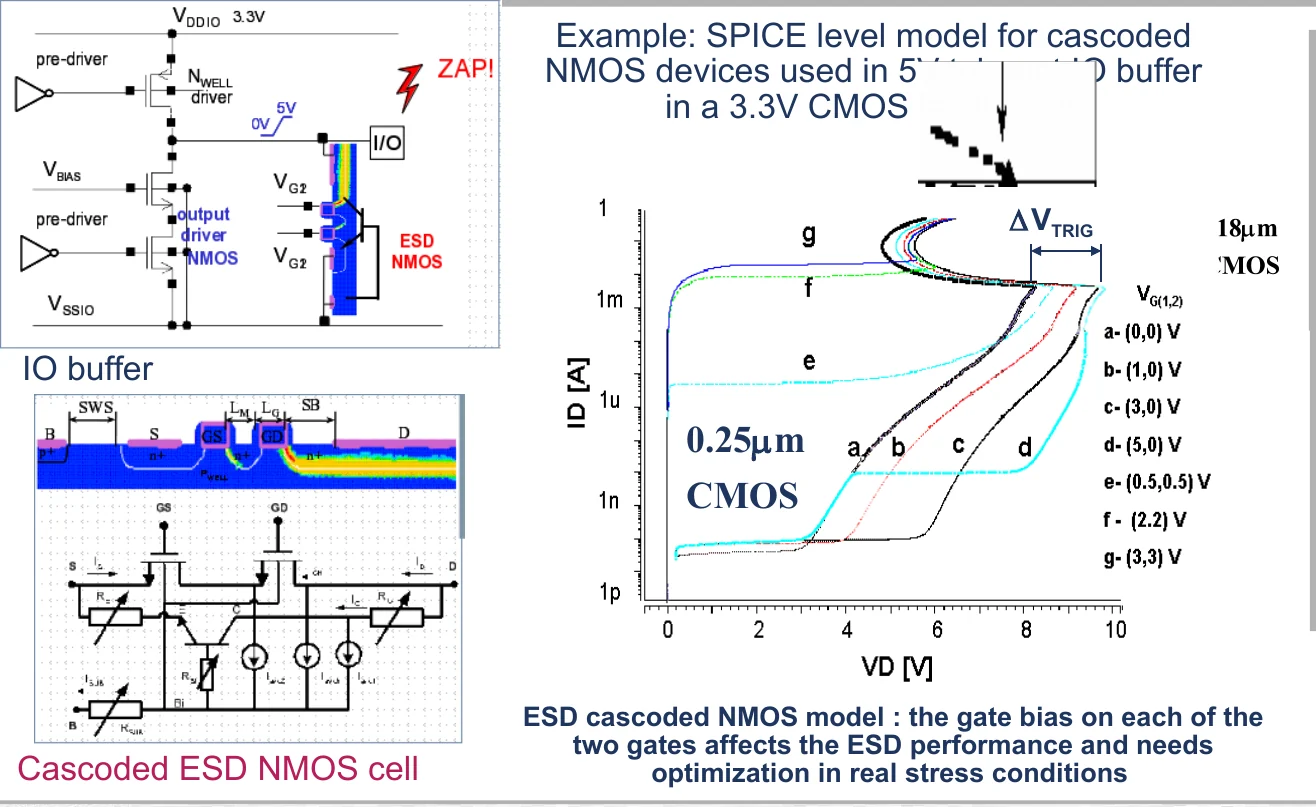
A SPICE-level model of cascoded ESD NMOS devices shows how the bias on each of the two gates shifts trigger voltage and has to be optimized under real stress conditions.
ESD protection for RF inputs
RF
Low-noise amplifier
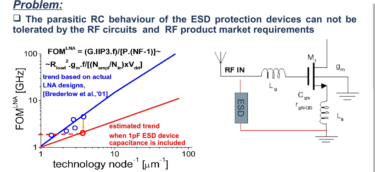
The parasitic capacitance of an ESD device lowers amplifier performance. Choosing between ‘plug and play’ and ESD–RF co-design depends on the RF spec and design space.
ESD device for a rad-hard test chip
Space
UMC 180 nm DARE
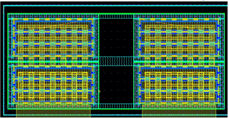
Layout and schematic of an ESD device implemented in a UMC 180 nm DARE test chip for ESA-approved rad-hard library development, in collaboration with IMEC.
Tell us about your ESD challenge
Send a short description of your technology, product or failure and we will tell you how we would approach it.