Home / Services / IC qualification and ESD troubleshooting

IC qualification and ESD troubleshooting

When a product fails ESD qualification or returns from the field, we find the root cause, define the design fix and verify it.

What we do

Troubleshooting works best when failure data, simulation and layout are looked at together. That is how we avoid trial-and-error redesigns.

  • IC qualification for ESD performance under HBM, CDM and IEC stress
  • ESD failure root-cause analysis and troubleshooting
  • Definition of design ESD fixes, verified in simulation
  • ESD performance improvement of existing IC products

Who this is for

IC product and reliability teams whose product shows ESD failures, or needs to qualify for HBM, CDM or IEC targets.
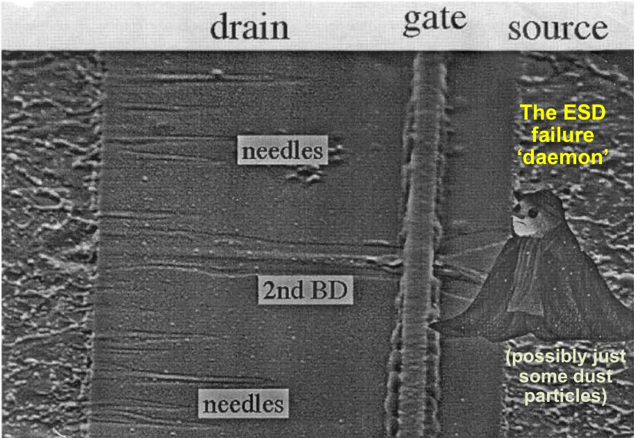
Electron microscope image of ESD damage in a MOSFET between drain, gate and source
A real physical-failure-analysis image of ESD-induced MOSFET degradation. Our simulation-based approach replaces ‘black magic’ with a model of what went wrong.

From failing curve to verified fix

Measure the failing behavior, reproduce it in simulation, change the design, and confirm the improvement. Two examples:
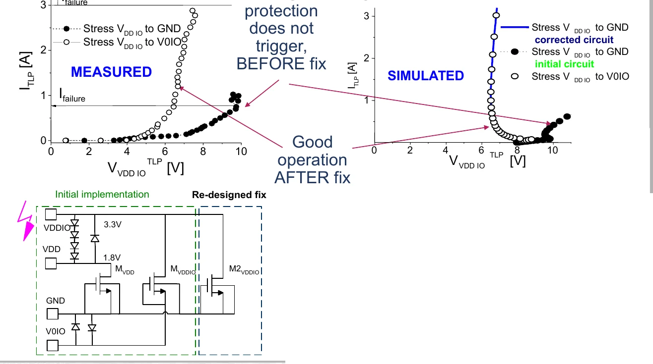
Power supply pad, protection does not trigger before the fix and works after
Power-supply pad: the protection does not trigger before the fix and works after the re-design.
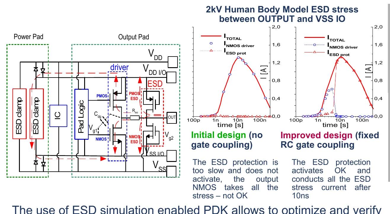
Digital output pad, too-slow protection before and RC gate coupling after
Digital output pad: the protection is too slow, so the output NMOS takes the stress. RC gate coupling fixes it.
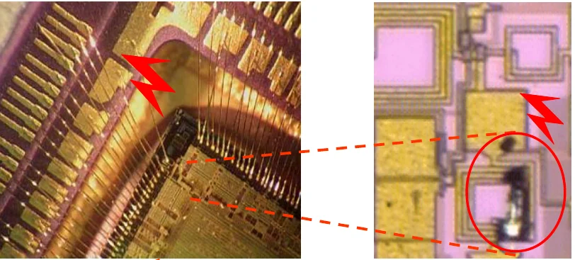
Photographs of a packaged chip and a close-up of a failed ESD protection structure
Chip-level failure due to an ESD event.

Tell us about your ESD challenge

Send a short description of your technology, product or failure and we will tell you how we would approach it.