
What we do
ESD structures, circuit definition and layout are designed together with your functionality, then simulated against the stress mode you target: HBM, MM, CDM or IEC.
- Design and qualification of ESD design library cells and IP for your silicon technology, CMOS or bipolar
- Design, implementation and review of dedicated ESD protection circuits for ASIC, SoC, analog, RF and automotive applications
- ESD–IC functionality co-design for digital, analog and RF blocks and for the full IC
- ESD design rule development for your technology
Who this is for
IC library vendors and design houses building digital, mixed-signal, RF, high-voltage or space products.
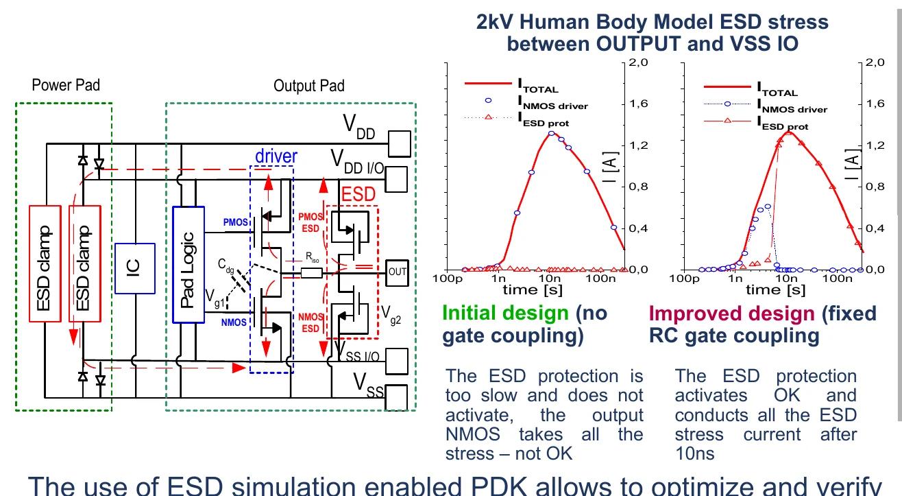
Application areas
Each application has its own ESD design window. We choose the protection approach that fits it.
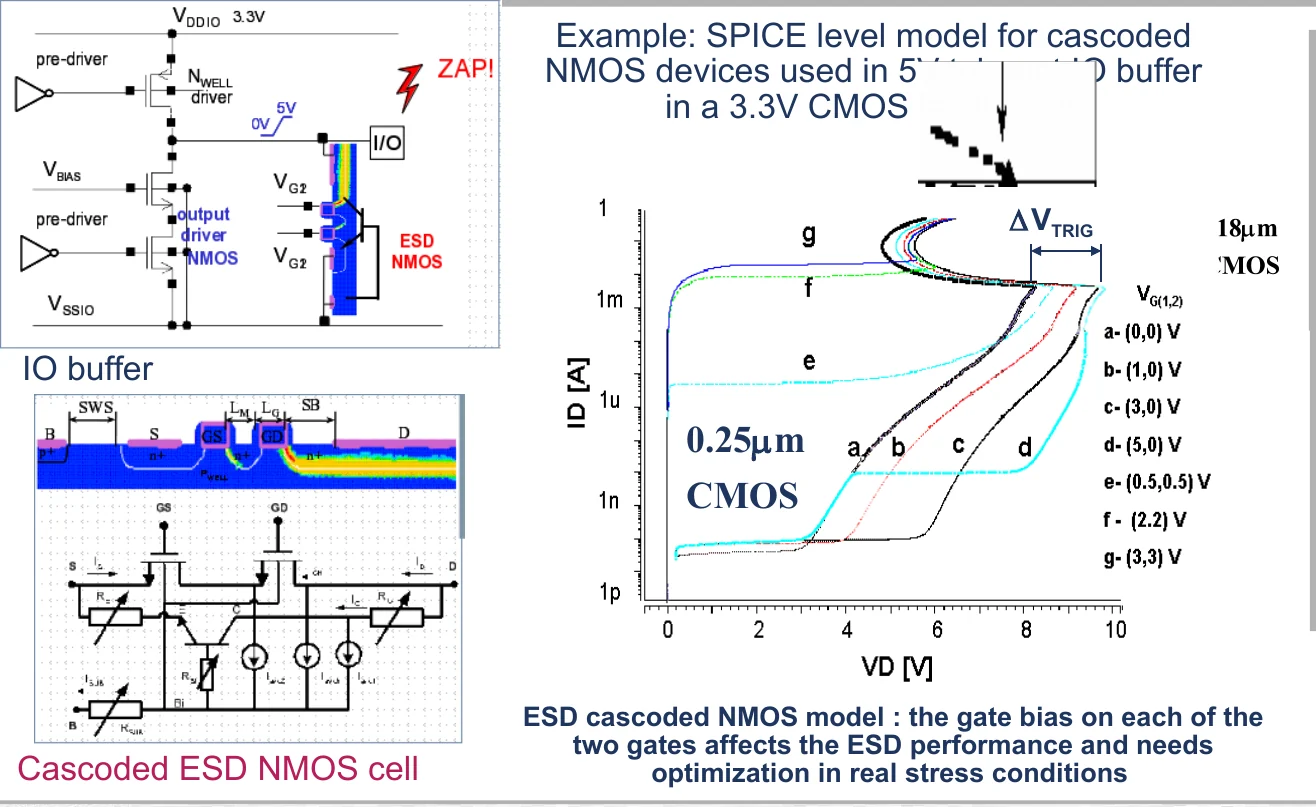
Mixed-signal and tolerant I/O
Cascoded ESD NMOS devices protect a 5 V-tolerant I/O buffer in a 3.3 V CMOS process. The gate bias on each of the two gates changes the ESD performance and has to be optimized under real stress conditions.
RF I/O
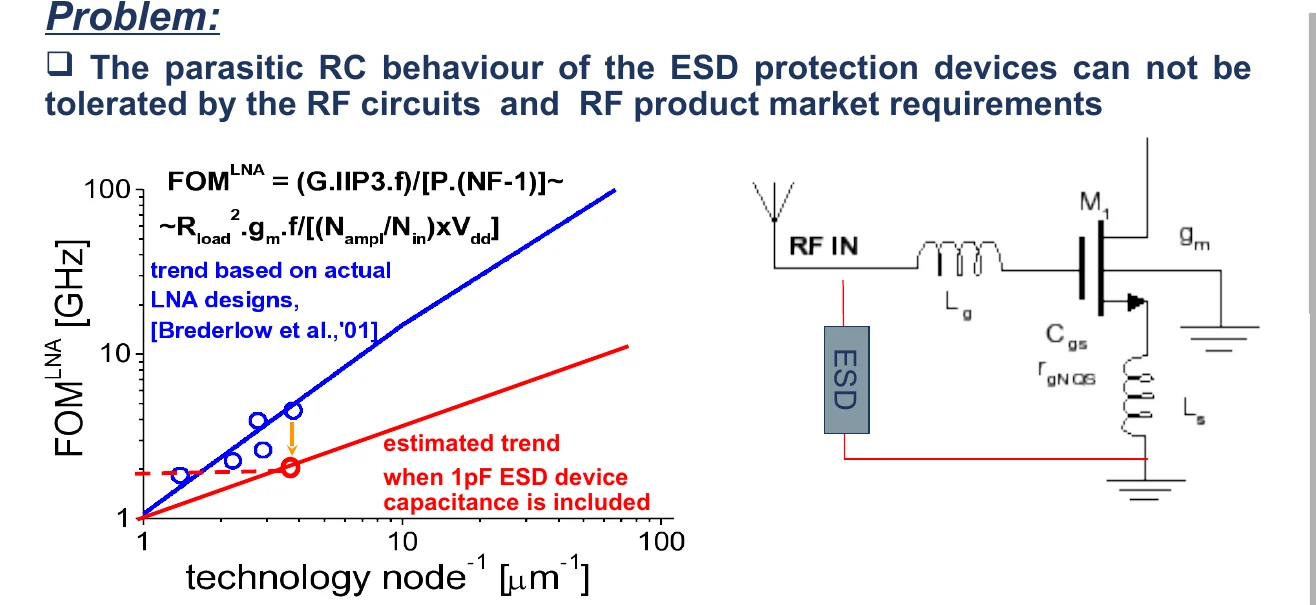
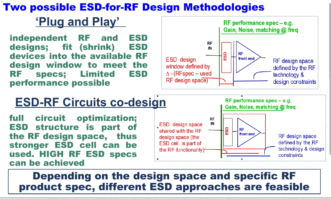
The parasitic RC of ESD devices reduces gain and raises noise. With ‘plug and play’ you fit a small ESD device into the available RF window and accept limited ESD performance. With ESD–RF co-design the ESD cell becomes part of the RF circuit, so a stronger cell can be used and high RF ESD specs can be met.
High-voltage and automotive
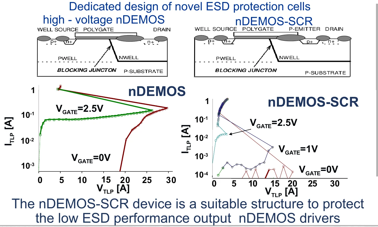
Protecting open-drain high-voltage drivers is hard because the ESD design window is small: no stress current may enter the nDEMOS output driver. We design and model dedicated cells such as the nDEMOS-SCR, whose trigger voltage drops from about 25 V to about 5 V when gate bias is coupled in.
Tell us about your ESD challenge
Send a short description of your technology, product or failure and we will tell you how we would approach it.